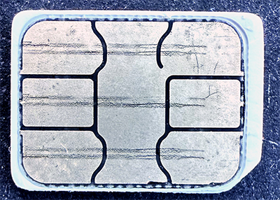
If one word could sum up what drives microscopy enthusiasts to explore the macro and micro world around them it is probably curiosity. It certainly is for me since my early teens (now in late 60s). So when a phone required a new SIM card the old one obviously offered the opportunity to explore inside. SIMs have reduced in size since their first use and are now in the tiny nano size.
I will leave others wishing to investigate to decide how to safely expose the chip but suggest any sharp knives used are always pressed down onto a non-slip craft pad and never towards the fingers. On removing the white plastic outer cover an inner chip cover was black plastic, this softened somewhat in toluene but required a sharp knife to nibble away. Below this was what looked like an epoxy type glue covering of the chip and again needed the same procedure. The chip was protected with a softer yellow covering which flaked away readily avoiding damage to the chip surface. Long exposure to a powerful solvent may remove these layers without recourse to a knife but I was eager to see the chip (short exposures in both acetone or toluene had little observable effect).
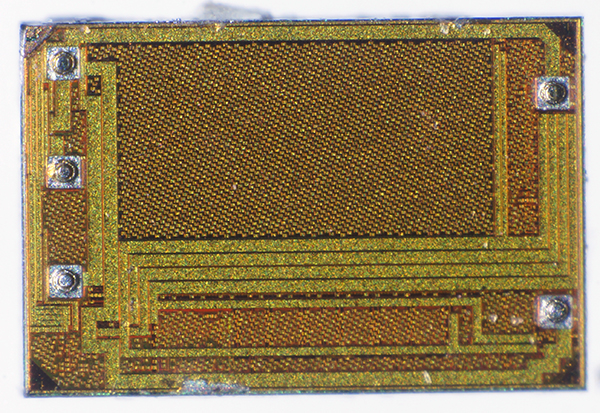
The chip was 1.43 x 0.93 mm in size. The gross features can be studied under the stereo but such subjects are also ideally suited for epi-DIC, in my case on a Zeiss Photomicroscope III.

Its macro layout was identical to a so-called EMV chip in the book 'Open Circuits' by Schlaepfer and Oskay of an exposed credit card chip including the glass fibre weave backing.
Stereo microscope image with ring lighting.
The chip was connected to the connecting pads by five wires, these were lost during dismantling but the pegs on the chip can be seen.
Zeiss incident epi-DIC 4X objective. The SIM has both passive and active features but the uniformity of the view on this outer layer suggested no active components in this layer.
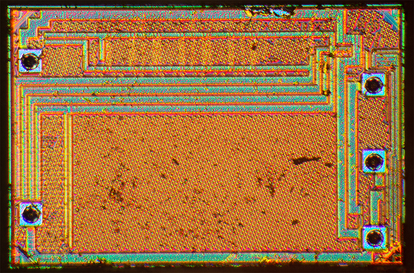
The interesting active component layers presumably lie within. The underside was just a featureless opaque glassy layer.
I posted the images in the Facebook group 'I Take Pictures of Electronic Parts'. Some responders with technical expertise generously offered explanations of what was visible and how the chips are typically constructed. Readers may wish to follow the thread rather than an attempt at paraphrasing what do not fully understand!
Images below with a Zeiss 40X epi-DIC objective.
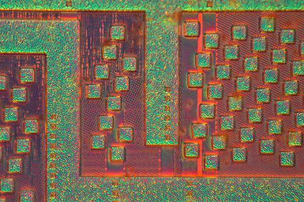
The square features were 0.0096 mm in width.
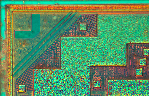
Corner detail. Sometimes chips have codes etched on but none were found on this layer.
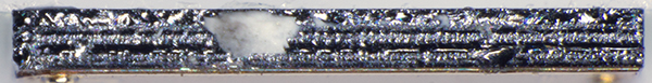
The tiny chip was supported on its side against a dampened glass slide edge which held it in place. The chip seems to be made of multiple layers of electronics.
I was aware that modern computer boards had multiple planes of components (and is the featured cross sectional image on the cover of 'Open Circuits' mentioned above) but did not realise such a tiny chip would also have such a construction.
Comments to the author David Walker are welcomed.